IFritz 5-Pulser
This circuit is a voltage-controlled waveshaper that produces a train of output pulses
that may be variedin number, width and position in response to a control voltage.
When fed with a sawtooth waveform,the pulses evolve from a single square wave to a train of five pulses occupying half a period or less of the output waveform.
The circuit is built around a LM3914 LED display driver chip, which simplifies the design of the pulse generation circuitry.
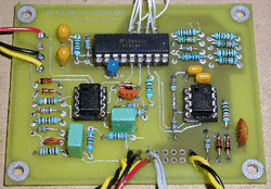
Component Placement and I/O connections
I/O Connector J2 Pinout:
Pin# Connection Pin# Connection
1 Sig. in (+/- 5 V) 2 Gnd (Twist with Sig. in)
3 +12 V: R5(1) 4 Shape: R5(2)
5 Gnd: R5(3), R8(3) 6 Mod: R8(2)
7 Gnd 8 Gnd
9 Gnd 10 Gnd
11 Gnd 12 Gnd
13 Gnd 14 Gnd
15 Sig. out 16 Gnd (Twist with Sig. out)
Note: On pots, (1) is CW, (2) is slider, (3) is CCW
Switch/Jumper J3 Pinout:
Pin# Connection Pin# Connection
1 S1 send 2 S1 retn. (Or jumper1-2)
3 S2 send 4 S2 retn. (Or jumper 3-4)
5 S3 send 6 S3 retn. (Or jumper 5-6)
7 S4 send 8 S4 retn. (Or jumper 7-8)
Pin# Connection Pin# Connection
1 Sig. in (+/- 5 V) 2 Gnd (Twist with Sig. in)
3 +12 V: R5(1) 4 Shape: R5(2)
5 Gnd: R5(3), R8(3) 6 Mod: R8(2)
7 Gnd 8 Gnd
9 Gnd 10 Gnd
11 Gnd 12 Gnd
13 Gnd 14 Gnd
15 Sig. out 16 Gnd (Twist with Sig. out)
Note: On pots, (1) is CW, (2) is slider, (3) is CCW
Switch/Jumper J3 Pinout:
Pin# Connection Pin# Connection
1 S1 send 2 S1 retn. (Or jumper1-2)
3 S2 send 4 S2 retn. (Or jumper 3-4)
5 S3 send 6 S3 retn. (Or jumper 5-6)
7 S4 send 8 S4 retn. (Or jumper 7-8)
Component List
ICs:
U1 TL072 (or similar) dual opamp
U2 LM3914 bar-graph driver
U3 TL071 (or similar) single opamp
Diodes:
D1, D2 1N4148 (or similar) switching diode
D3, D4, D5 1N751A (or equivalent) 5.1 V Zener diode
Resistors (all metal film 5%):
R33 1 kOhm
R32 2.2 kOhm
R11, R30 3.9 kOhm
R12 5.6 kOhm
R20, R22, R24, R26 10 kOhm
R28 "
R2, R4, R31 22 kOhm
R7, R9, R10 82 kOhm
R21 120 kOhm
R23, R25, R27, R29 150 kOhm
R6 200 kOhm
R1, R3 220 kOhm
Pots:
R5, R8 100 kOhm
Caps:
C2 10 pF 10% ceramic
C4 56 pF 10% ceramic
C5 .01 uF 10% ceramic or poly
C9, C10 .1 uF ceramic or poly bypass
C1, C3 .47 uF poly
C8 2.2 uF electrolytic bypass
C6, C7 4.7 uF electrolytic bypass
Circuit
